



You're probably in a review meeting with one question hanging over the table, can this next device really use a polymer where the team usually reaches for indium tin oxide, copper, or a metal mesh? That question comes up because conductive polymers are rarely chosen to beat metals at their own game. They're chosen when the product needs to bend, print at low temperature, stay light, or interact safely with tissue, and that changes the whole selection logic.
The commercial picture is already broad. Industry and review sources describe conductive polymers as established in antistatic materials, commercial displays, and batteries, while newer uses keep expanding into organic solar cells, printed circuits, OLEDs, chemical sensors, biosensors, electromagnetic shielding, and flexible transparent displays (Scientific American topic overview on conductive polymers). Market forecasts in the brief also show that this is no longer a niche lab category, it's a multibillion-dollar material class with demand anchored in electronics, energy, and wearables (Research and Markets conductive polymers market report).
The practical job is simple to state and hard to do well. Map the device requirement to the material role, then decide whether a conductive polymer should be the electrode, coating, sensing layer, shielding layer, or active interface. That's a better starting point than asking whether the polymer is “as conductive as metal,” because in many conductive polymer applications, conductivity is only one part of the decision.
Table of Contents
- Doping is the lever, not a side note
- Percolation explains why the jump can feel sudden
- Why three names keep coming up
Why Conductive Polymers Earn a Spot in Modern R&D
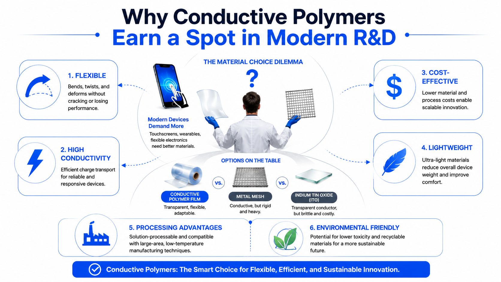
A formulation team gets a prototype on the bench, and the constraint list starts to pile up. The display stack needs transparency, the housing cannot crack under bending, the process has to stay at low temperatures, and the device still has to move charge reliably. At that point, the team stops asking whether a polymer can replace a metal and starts asking where a conductive polymer can do a better job than a rigid conductor.
Where the first wins usually appear
The first wins usually show up in transparent electrodes, antistatic coatings, flexible interconnects, and printed layers where low-temperature processing matters. PEDOT:PSS is a common choice in those roles because it can be solution processed and tuned for conductivity while still keeping optical clarity, so it appears often in flexible electronics and OLED-related layers (Nature article on PEDOT:PSS). The same pattern appears in market reporting, where the electrical and electronics segment holds 41.6% of the conductive polymers market in 2025 in one forecast, and 41.60% of end-use demand in 2025 in another (2025 market forecast, 2025 end-use market forecast).
Practical rule: if the part has to bend, print, coat, or interface with tissue, the polymer is often chosen first for the process window, then for the conductivity.
The six families worth tracking
The field becomes easier to manage when you group it into six application families. Those families are electronics, energy storage, sensors, biomedical devices, coatings and shielding, and the formulation and scale-up workflow that makes the first five commercially viable. A table helps show where conductive polymers already win in practice.
| Application Family | Typical Polymer | Why a Polymer Works Here |
|---|---|---|
| Flexible displays and transparent electrodes | PEDOT:PSS | Printable, transparent, flexible |
| Antistatic coatings and ESD layers | PEDOT:PSS, PANI | Thin-film coating, tunable conductivity |
| Batteries and capacitors | PEDOT derivatives, PANI, PPy | Charge transport with low-temperature processing |
| Sensors and wearables | PPy, PANI, PEDOT:PSS | Mechanical compliance and stable electrical response |
| Biomedical interfaces | PPy, PANI, PEDOT:PSS | Tissue-like mechanics and biocompatibility |
| EMI and shielding coatings | Conductive polymers and composites | Light weight, conformal coating, processability |
The market outlook backs up that spread. One 2025 report values the global conductive polymers market at USD 4.7 billion in 2025 and projects USD 9.9 billion by 2034 at an 8.5% CAGR, with automotive/e-mobility growing fastest at 9.18% CAGR through 2031 (2025 market forecast). Another forecast places the market at USD 5.9 billion in 2026 and USD 8.77 billion by 2031, with product components at 44.05% of market size in 2025, as noted earlier (2025 end-use market forecast).
The selection mindset matters more than memorizing a material list. R&D leaders who win here do not ask which conductive polymer is “best” in the abstract. They ask which one can survive the actual device stack, the actual process sequence, and the actual failure mode. That is why AI platforms like Polymerize matter across these use cases, they shorten the trial-and-error loop by helping teams compare formulations, processing windows, and performance trade-offs before a full round of lab work.
The Core Concept Behind Polymer Conductivity
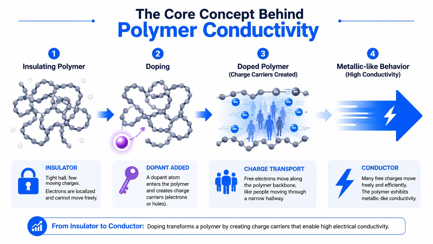
A polymer begins as an insulator because its electrons are tied to the backbone and do not move freely the way they do in a metal. Doping changes that balance. The backbone still provides the structure, but the dopant introduces mobile charge carriers, so a material that once blocked charge can start to carry it in a controlled way.
Doping is the lever, not a side note
Conductive polymers do not sit at one fixed conductivity. Their behavior can move from insulating to metallic-like as the doping level changes, and that tunability is the main control knob in formulation work. In practice, increasing dopant content can raise conductivity, but it can also disturb film morphology, reduce transparency, or weaken mechanical integrity. Materials teams spend so much time on secondary additives and post-treatment because the base resin rarely delivers the full mix of electrical, optical, and mechanical performance on its own.
Rule of thumb: every conductivity gain should be checked against three losses, optical clarity, flexibility, and process stability.
Percolation explains why the jump can feel sudden
The percolation threshold is the point where isolated conductive regions begin to connect into one continuous pathway. Before that point, the film behaves like a road network made of disconnected streets and dead ends. After that point, charge can travel across the film with much less resistance. That is why some formulations seem disappointing until they cross a specific structural threshold.
PEDOT:PSS is a clear example of this tuning logic because it combines solution processability with a wide conductivity window and practical value in antistatic and transparent-electrode roles, as discussed in the Nature article on PEDOT:PSS. PPy and PANI matter for the same reason in different use cases. They give R&D teams enough design space for sensors, flexible layers, and biomedical interfaces without forcing high-temperature processing or rigid device stacks.
Why three names keep coming up
The application literature keeps returning to PEDOT:PSS, polyaniline, and polypyrrole because they cover different corners of the same design space. PEDOT:PSS is the easiest to process in solution. PANI is attractive where electrochemical response and stretchable sensing matter. PPy often appears where actuation, sensing, and biointerface behavior need to work together, as summarized by CAS Insights on conductive polymers.
That mix is why conductive polymer applications are so broad. These materials are not one thing. They are tunable platforms whose conductivity, mechanics, and chemistry can be adjusted like separate controls on an instrument panel, which is exactly why they earn a place in devices where metals or carbons are too rigid, too harsh to process, or too hard to match to biological tissue.
Electronics and Energy Storage in Practice
Electronics is where conductive polymers first proved they could earn a place in commercial devices, and energy storage is where they keep showing why that place matters. The shared advantage is not sheer conductivity. It is the ability to move charge in forms that metals handle poorly, such as transparent films, conformal coatings, and layers that can be printed at low temperature.
In devices, the polymer role is often structural
PEDOT:PSS appears repeatedly in displays, OLED-related layers, touch interfaces, and printed circuits because it can serve as a transparent conductive layer without the brittleness of a metal mesh or an indium tin oxide-like stack. In antistatic and ESD work, the goal is usually to bleed charge away safely rather than carry high current, so a thin conductive coating is enough. A polymer can win on practicality here even if it does not match a metal on maximum conductivity.
The same logic applies in EMI shielding. A lightweight coating that follows the shape of a housing, a cable, or a textile can be more useful than a rigid metal shield when the geometry is irregular. Polyaniline also remains relevant in coating and sensing roles because it can be tuned for electrochemical behavior and processed into layers that are easier to integrate than a metal foil.
Energy storage rewards interface control
In batteries and capacitors, conductive polymers are useful as functional layers, composite electrodes, or conductive binders where low-temperature processing and interface quality matter. As noted in the market overview, demand is concentrated in uses such as capacitors, batteries, ESD/EMI shielding, printed circuit boards, and sensors. That pattern points to a clear role for the polymer. It often handles interface work, while the active electrode does the heavy lifting.
Practical insight: if an energy-storage design needs a flexible current pathway, a printable layer, or a coating that survives gentle processing, the polymer may be the better tool even when its intrinsic conductivity is not the highest in the stack.
A useful way to sort the electronics use cases is by what the part must preserve. Transparent electrodes preserve optics. Printed interconnects preserve manufacturability. Antistatic layers preserve safety. Energy-storage layers preserve contact and ion transport at the interface. Those are different engineering jobs, and conductive polymers are rarely chosen for the same reason in each one.
The market concentration reflects that breadth. As noted earlier, the electrical and electronics segment dominates demand because flexibility, processability, and charge transport collide most often.
Sensors, Biomedical Devices, and Wearable Interfaces
Sensors expose the trade-off between conductivity and mechanics very clearly. A device that works on the benchtop but loses contact after a few flex cycles is not a product. In wearables and biomedical devices, the material has to keep an electrical interface alive while the body, fabric, or substrate keeps moving.
The body rewards compliance, not stiffness
Reviews in the brief identify PPy, PANI, and PEDOT:PSS as the main biomedical workhorses because they combine electrical conductivity, flexibility, and biocompatibility for biosensors, neural interfaces, tissue-engineering scaffolds, and controlled stimulation platforms. CAS Insights on conductive polymers captures that pattern well. The reason is straightforward. A soft interface that follows tissue motion often performs better in real use than a harder material that resists deformation but later lifts or delaminates.
Flexible and stretchable devices use conductive-polymer films as electrodes or active layers for strain, temperature, gas, and health-monitoring sensors. The design problem is not just making the film more conductive. It is keeping the film attached, stretched, and electrochemically stable while the device bends and relaxes again and again.
The best analogy is a spring contact in a moving assembly. If the contact only works while perfectly aligned, it fails in service. Conductive polymers are attractive because they can keep that contact alive while the surrounding structure changes shape.
Key insight: in wearables, a slightly less conductive film that survives motion is usually more valuable than a highly conductive film that cracks.
Why the same family shows up in very different devices
A chemical sensor, a neural interface, and a stretch sensor do not ask for the same balance of properties. A chemical or biosensor may prioritize surface chemistry and stable signal transduction. A neural interface needs a steady electrical interface and tissue compatibility. A stretch sensor needs elongation without signal collapse. Conductive polymers are useful because their chemistry can be adjusted across that range.
The practical design rule is to balance conductivity, elongation, adhesion, and electrochemical stability rather than chase conductivity alone. That is the part that often gets missed in early development. Failure usually starts at the interface, not in bulk resistivity.
The wearable market keeps pulling these materials into new formats because textiles, patches, and soft electronics all benefit from a conductor that can live where metal is too stiff. PPy, PANI, and PEDOT:PSS each sit in different corners of that space, but the selection logic stays the same. Start with the body, the substrate, and the motion profile, then choose the polymer that can stay functional in that environment.
As product teams move from lab samples to repeated use, tools like Polymerize can shorten the trial-and-error loop across these formats, surfacing which chemistry and process window are most likely to survive the motion, contact, and adhesion demands.
Coatings, Composites, and the Honest Trade-Offs
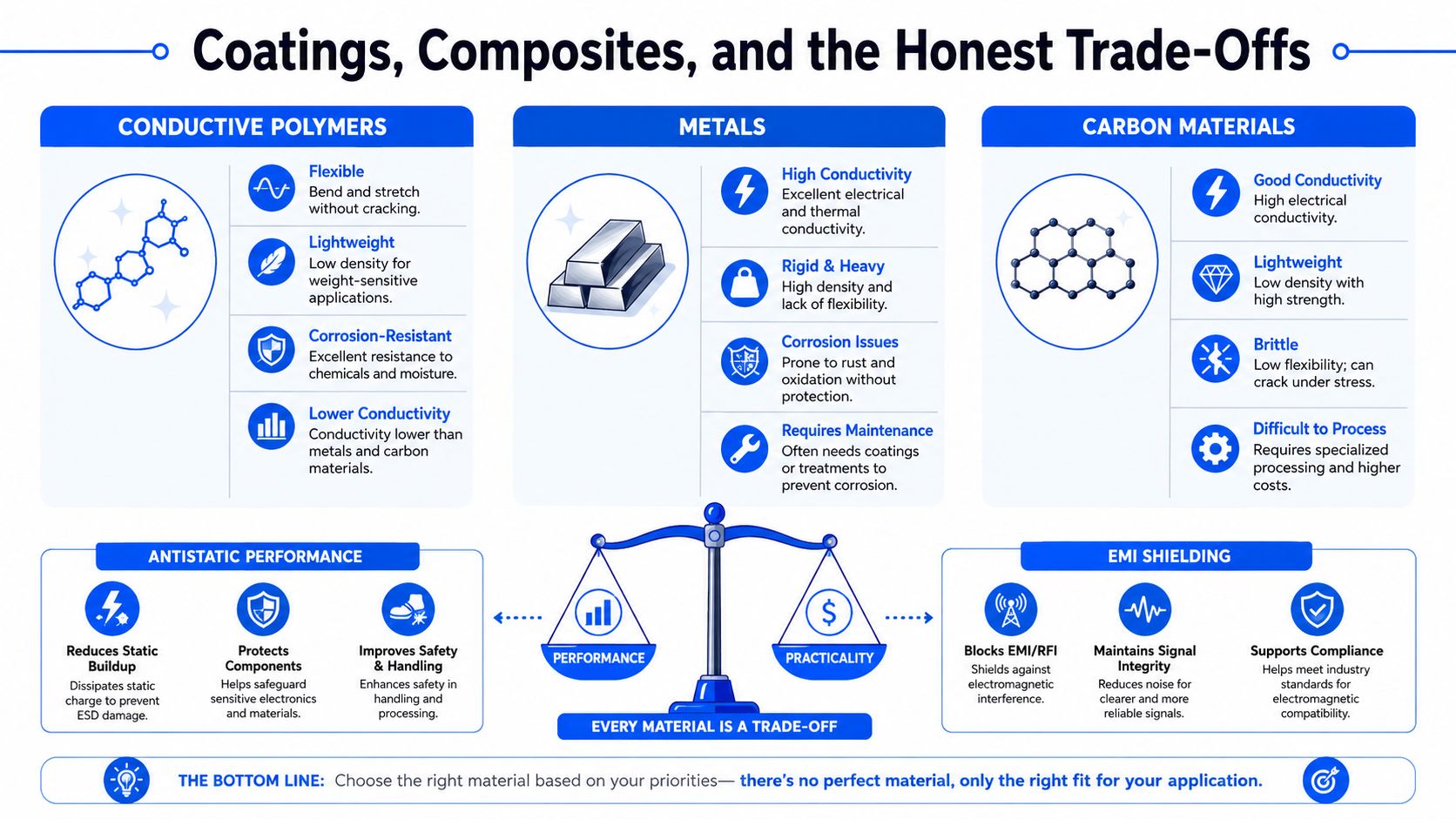
Conductive polymers win most clearly when the product needs a coating or composite, not a bulk conductor. That is where they can beat metals, carbon materials, and conventional polymer coatings on manufacturability, weight, and shape conformity. They also lose in places where people sometimes expect them to win, which is why honest trade-offs matter.
Where polymers clearly beat the alternatives
For antistatic and EMI shielding coatings, a conductive polymer can give you a conformal, light, low-temperature process that fits complex geometry better than a metal film. That matters on housings, enclosures, textiles, and soft devices where a rigid conductor creates handling or cracking problems. In corrosion-prone environments, the polymer coating can also provide a more forgiving interface than bare metal if the application doesn't require extreme conductivity.
Composite systems are another strong case. Conductive polymers can be combined with carbon or metal additives to create hybrid coatings and films that balance conductivity and processability. The value of the polymer in those systems is often to create a continuous film, improve adhesion, or bridge gaps between filler particles. The filler provides the electrical backbone, while the polymer handles the coating mechanics.
Where they lose, and that's okay
They are not the right answer when the job is to maximize conductivity above everything else. They also struggle in some harsh chemical environments and in long-term thermal cycling where a metal or ceramic-based system may be more reliable. The contrarian point is worth stating plainly, conductive polymers are often not the highest-conductivity choice, and they shouldn't be treated as if they are.
Independent review coverage in the brief says conductive polymers are widely used in energy storage, sensing, coatings, and biomedical devices, while also emphasizing practical limitations and the need for further development before broader adoption in some uses (PMC review on conductive polymers). That's the correct framing for R&D. Use the polymer when flexibility, low-temperature processing, tunable chemistry, lightweight design, or biocompatibility matters more than peak conductivity.
Decision framework: choose the polymer when the product is constrained by form factor, process temperature, or interface biology. Choose metal or carbon when the only thing that matters is moving electrons as efficiently as possible.
That framework helps teams avoid false substitution thinking. A conductive polymer is not a defective metal. It's a different engineering material with a different win condition. Once that's clear, the design conversation gets much sharper.
Selecting and Processing Conductive Polymers at Scale
The lab-to-production gap is where many conductive polymer programs slow down. A material can look promising in a small coating test and still fail once the team asks it to survive drying, printing, adhesion checks, humidity, or a real substrate. Scale is less about one magical formulation and more about controlling a chain of small decisions.
Start with the property that can't move
The first question is what cannot change in the final part. If transparency is fixed, you cannot solve conductivity by loading the formulation with too much additive. If flexibility is fixed, you can't choose a brittle film and hope the device packaging saves it. If the substrate is heat-sensitive, low-temperature processing becomes essential.
Secondary doping is one of the central levers for PEDOT:PSS, PANI, and PPy, and it changes conductivity by altering polymer conformation and charge transport pathways (Patsnap survey on PEDOT:PSS and PANI). That makes dopant choice and additive system selection more than a chemistry detail. They directly influence film morphology, conductivity, and mechanical strength.
Watch the failure modes before you scale
The most common scale-up problems are not exotic. They're batch-to-batch conductivity drift, adhesion loss, and stability failures under heat or humidity. Those problems often come from dispersion, drying, or substrate mismatch rather than the polymer backbone itself. A film that looks uniform in a small dish can behave very differently when coating speed, drying rate, or line tension changes.
A simple development checklist helps:
- Define the use window first: set the minimum conductivity, allowed thickness, and bend or stretch target before you choose a formulation.
- Test adhesion early: check whether the film stays attached to the actual substrate, not just to a convenient lab coupon.
- Run environmental stress quickly: humidity and thermal exposure often expose weak formulations before electrical testing does.
- Track morphology, not just resistivity: a stable structure usually predicts a more stable product than a single resistance measurement.
If your team is managing many formulation variants across notebooks, ELNs, and pilot batches, an AI-native system such as Polymerize can centralize the data, connect formulation choices to property outcomes, and help surface the next experiment from the data already on hand.
How AI Systems Like Polymerize Accelerate Conductive Polymer R&D
Conductive polymer work generates a lot of useful data, but much of it stays trapped in spreadsheets, lab notebooks, or ELNs. That creates a familiar problem. A scientist knows the team has already tested something close to the next idea, but finding the exact run, the exact substrate, and the exact additive level takes too long. The result is avoidable trial and error.
Data unification changes the starting line
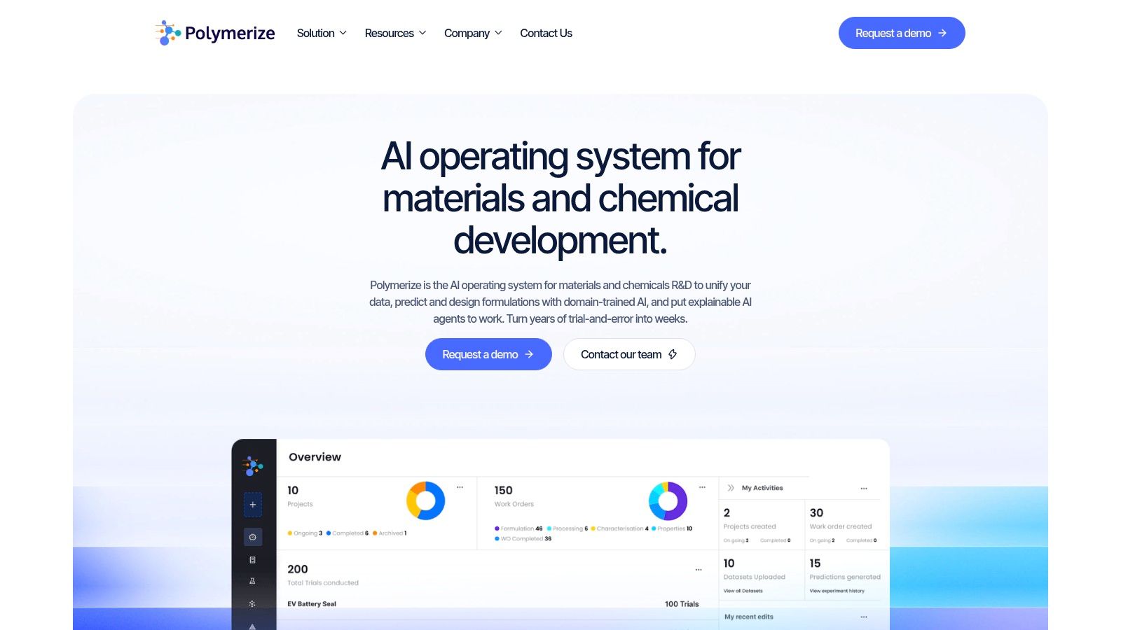
An AI-native materials intelligence platform begins by pulling fragmented experimental data into one secure backbone. That matters because conductive polymer formulation is a relational problem. Conductivity depends on dopant choice, solvent system, additive level, substrate, and drying history at the same time. Once those variables are organized, model training becomes possible instead of guesswork.
The value is not just storage. Domain-specific, explainable models can predict properties, optimize formulations, and surface causal drivers with confidence scores and historical precedents, so the scientist can plan the next best experiment rather than repeat dead ends. In conductive polymer work, that means fewer blind formulation loops and faster movement from screening to a validated process.
The real payoff is shorter iteration cycles
The best AI workflow does not replace the formulation chemist. It compresses the path from hypothesis to result. A materials team can compare likely conductivity, stability, and morphology outcomes before running the batch, then use the result to refine the next round. That is especially useful in this topic because the trade-offs are real and unavoidable. If you raise conductivity, you may hurt transparency or flexibility. If you improve stretchability, you may lose some electrical performance.
Video can also help teams align on the workflow.
Expert-supported programs and prototyping networks can then carry the best candidates from lab formulation to validated material, which is the point where many conductive polymer programs stall. That closes the loop across discovery, screening, and scale-up, and it gives R&D leaders a clearer route to ROI on materials AI investment. The practical gain is fewer failed experiments, faster scale-up from lab to production, and a tighter connection between application need and formulation choice.
If you're trying to choose the right conductive polymer for a display, sensor, coating, or wearable, Polymerize helps organize the formulation data, predict properties, and guide the next experiment instead of leaving the team stuck in manual trial and error. Visit Polymerize to see how an AI-native materials R&D platform can support conductive polymer development from first screening to scale-up.
Put your R&D data to work
See how materials teams use Polymerize to plan fewer experiments and reach target properties faster.